Coarse approach

IMG_2873

I recently motorized the coarse approach mechanism on my STM. The coarse approach is done by first fully extending the Z-piezo (reasonably slowly) to search for the surface. If it doesn’t find the surface, it fully retracts, and a stepper motor, which drives the rear fine-pitch screw on the STM, takes a few steps to move the tip close to the sample. The distance it moves is somewhat less than the Z-piezo travel. After moving the motor, the Z-piezo fully extends again to search for the sample surface. This process repeats until the piezo finds the surface. When this happens, the Z-piezo retracts one more time, and the motor adjusts the piezo height above the sample so that, when the scanner extends one last time, it will find the sample at about the center of its travel range (just to give it some room to drift in either direction). Once the sample surface is found the Z-feedback loop switches on, and scanning begins.

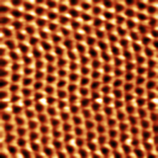
Here are some images zooming in on a gold surface taken after doing a motorized coarse approach. Note the lack of craters! I’ve applied some lighting effects in Gwyddion to help make the edges of the atomic terraces more apparent. No luck resolving individual atoms on metals yet though… I believe the issue is acoustic noise. Time to build a sound-proof box…

This technique is called the “woodpecker” approach, and it prevents vibrations from the motor from crashing the tip, since only the Z-piezo brings the tip and sample into contact. Since the hard part is done by the piezo, the motor step size only needs to be smaller than the piezo range, although it’s nice to have a smaller step size to be able to center the scanner in its travel range before beginning the scan.

My scanner has about 700 nm vertical travel. Creating steps much smaller than this with a stepper motor is really no problem at all, especially since we don’t care about backlash. I used the 28byj-48 stepper motor to drive the rear fine-pitch screw on the STM. I milled a slot in the end of the screw’s plastic knob that fits over the motor shaft, while allowing the screw to move up and down. The 28byj-48 motor is very cheap and is geared down to about 2048 full steps/revolution. The fine screw moves 250 um/revolution, and the STM body’s lever reduction reduces the motion by a factor of about 20. This gives a step size of 250um/2048/20 = 6 nm.

IMG_2871

There are a few subtleties that came up here: when the Z-feedback is switched on, the integral term first must be initialized to the current Z-value. Otherwise, the feedback will cause a small jump in the Z-piezo when it’s switched on, which crashes the tip! Took me a while to figure out why I was still seeing craters in my scans! Another issue is thermal drift. The motor produces a substantial amount of heat, which can cause the scanner to drift out of range within minutes. The solution is simply to turn the motor off when it’s not moving, i.e. when the piezo is extending and when the scan starts. This means that we can’t use microstepping, which is I used a geared motor in the first place. I’m also running the motor on 3.3V rather than 5V to further reduce heating.

STM software

software

I finally got around to finishing up the Teensy software for my STM! The Teensy controls scanning, PI control of the Z-axis piezo, sigma-delta modulation of the scanner DAC outputs, and serial communications with a PC. I also wrote a C# program (screenshot above) that receives the serial data sent by the Teensy and displays the images line by line, and can set the scan parameters.

Here are the files:

There are simple libraries for the DAC8814 and LTC2623-16 included with Teensy software. Put them in your \Arduino\libraries folder. The PC software contains a .exe file and .exe.config file. Just put them in the same folder somewhere.

I’ll do a more detailed writeup on this later, but here’s a brief summary of how it works: the Teensy uses a timer to call a function at a regular time interval. This function increments the scan, performs PI calculations to update the Z axis, and performs sigma-delta modulation of the scanner DACs. Since the scanning probe is a (sharp, fragile) solid object, it’s velocity needs to be controlled at all times. If it moves too fast, it will likely crash into something, so the tip scans in a zig-zag pattern rather than a traditional raster (as in a CRT or SEM for example). Since the STM is always incrementing the scan at the same time interval, doing a slower scan will acquire more data. All data acquired between pixels is averaged, so you’ll get less noise in a slower scan. Once a line of the image has been scanned in one direction and re-scanned in the other direction, the Teeny sends the Z data and error signal data over USB.

If you need to invert the Z-axis signal, find the “#define INVERT_Z true” at the top of the Teensy code and change it to false.

The PC software receives the data, does some basic processing, and adds it to the images on the screen. The left image is the topography (Z signal) and the right image is the error signal. The error signal looks like the gradient of the Z signal and has more high-frequency content. The topography data is displayed line by line in the graph at the bottom of the window. The red curve corresponds to the most recent scan line, and the blue curve is the same line scanned in the opposite direction. Ideally, these curves should be identical, but the agreement will never be perfect due to piezo hysteresis and things like that. If they don’t agree at all or show oscillations, try lowering the line rate, proportional and/or integral gains. For scans larger than ~500 nm or so, you’ll probably want to scan at ~0.5-2 Hz or so. For scans < 10 nm, you’ll want to go much faster to minimize thermal drift effect, ~10 Hz or more. You can also decrease the number of pixels to increase the speed.

Connect a LED to pin 0 on the Teensy. This is used to indicate serial communication is active. Connect another LED to pin 1. This one lights up when tunneling is achieved.

To use the software:

  1. Upload the code to the Teensy
  2. Turn the microscope on and start STM.exe
  3. Select the Teensy’s COM port from the list
  4. Do coarse approach until tunneling is achieved
  5. Press “Engage tip”. All this does at the moment is start the scan. You should see data coming in.

Images are saved as 16-bit, multi-page, uncompressed tiffs whenever a scan completes. You’ll want to use a program like Gwyddion to process the images, otherwise they’ll mostly just look gray. To view the error signal image (page 2 of the tiff), load the file into Gwyddion, click “Info” -> “Show Data Browser”, and check the box next to the error signal image.

There are still some issues in the PC software but it should work for the most part. It crashes on exiting, and I think I know what might be causing this but haven’t managed to fix it yet. I’ve also noticed that scan lines in the saved images are sometimes missing. CPU usage tends to be high when scanning at higher line rates. I’ll hopefully have a fix within a week or so and will update this post once I do.

If you find any other issues or have suggestions for improvements, please let me know in the comments!

Firmware improvements

scan_I_Au_600nm_1Hz_

I’m making some major changes to the Teensy firmware and wanted to share this image of a gold surface I took after making some improvements to the way the scan is generated. Previously, I was just advancing the scan in single pixels increments, but this produced relatively coarse motion which seemed to be causing spikes in the tunneling current during scanning, and possibly exciting scanner resonances.

I’m now advancing the scan in much smaller increments to provide smoother scanning motion, and averaging all the data acquired between pixels. So far, the results are looking pretty good! The above image is of the error signal, and it looks quite crisp and clean compared to most of my previous scans. Unfortunately I crashed this tip several times while debugging code, so smaller scans didn’t look quite as good, although I was still able to resolve atomic steps. The roughness in the upper right part of the image is likely the site of a tip crash. The weird mirror-effect on the left edge is due to an off-by-one error in the code somewhere…

I can also run faster scan rates now, up to about 40 Hz at 512 pixels per line, and faster at lower resolutions. This seems to be a little too fast for a disc scanner but should work well with the small tube scanner that I’ll be upgrading to soon. I’ll post the new code I’m working on soon.

New SPM design progress

I’m working on a new scan head design using a tube scanner and automated coarse approach. Still a work in progress, but here’s a look at what I’ve got at the moment:

STM_rev2

I’ve kept the 3-screw coarse approach mechanism since it’s compact and rigid. The tube scanner and approach screws are in the the lower part, and the tip and preamplifier in the upper part. This way, I can easily swap between STM and AFM heads (still a ways to go on the AFM part). The sample mounts to a magnet glued to the end of the tube scanner.

STM_rev2_2

The coarse approach mechanism has to be able to bring the tip within the tube scanner’s vertical travel range, so that the scanner can find the sample. This is done by stepping the approach motor, then extending the scanner to search for the sample surface. If it detects the surface, it starts scanning, otherwise the scanner retracts and the motor takes another step. This is called the “woodpecker” approach method, and it prevents tip damage since the motor and scanner are never moving at the same time.

STM_rev2_3I’ll be using the 28byj-48 stepper motors, since they are geared down to about 4096 steps/rev. Since these are dirt cheap, I might as well put one on each approach screw so the approach is always done vertically. The motors can be stepped sequentially to maximize resolution. Each motor drives a 3/16″-100 screw (moves 254 um/rev), so resolution will be 254 um /4096 / 3 = 21 nm steps. Not bad! I’ll probably full-step the motors to double the step size since this is smaller than necessary. Having a small step size makes it possible to center the scanner in its travel range after detecting the surface.

Piezo tube scanner

Got a tube scanner in the mail today! I paid $100 for it from Boston Piezo Optics, which seemed pretty good. If you want to get a tube from them, just make sure you get one that’s in stock as it will be much cheaper.

IMG_2264

As I am more interested in high resolution than large scan ranges, I got a small, rigid tube with 0.25″ OD, 0.50″ length, and 0.025″ wall thickness. Dielectric material is PZT-5A. I’m going to design a new scan head for it, and include a stepper motor-driven coarse approach mechanism. Of course, i’ll also need to build a high-voltage amplifier to drive the tube scanner.

So how will this compare to the unimorph disc? My disc scanner has about 700 nm Z-travel and 1700 nm XY-travel, and about a 3.4 kHz resonant frequency. The Z-axis displacement Δz of a tube scanner can be calculated as follows [1]:

\Delta z=\frac{d_{31} V L}{t}

where L is the length of the scanner (0.50″), d31 is the piezoelectric constant (173 pm/V for PZT-5A), V is the applied voltage, and t is the wall thickness. This gives about 1 um for my tube with a 250 V range. We can also calculate XY displacement:

\Delta x=\frac{0.9d_{31} V L^2}{t(ID+t)}

which gives 1.7 um for my tube, so in terms of range, this tube is pretty similar to the unimorph disc, but requires much higher voltages. The big difference is in rigidity. This tube should have an extensional resonant frequency around ~30 kHz for a 1 g load [2], which should give a huge improvement in terms of scan speed and vibration tolerance.

[1] EBL Products has some useful information on tube scanners, including material properties and displacement formulae.

[2] Tetsuo Hanaguri has a spreadsheet to calculate scan tube resonant frequencies.

MLCC piezo actuators

The unimorph disk scanner is cheap, has low capacitance, and works at low voltages, making it great for a low-cost SPM. It does have one major disadvantage though: poor rigidity, especially in the Z-axis where it’s most important. This makes it highly vulnerable to vibrations and limits scan speed.

I’d like to replace the unimorph disk scanner in my STM with something more rigid. I thought about using multilayer ceramic capacitors (MLCCs) as actuators, given that they’re piezoelectric. A quick google search turned up one article on the subject (journal article is here).

The authors were able to get displacements of ~500 – 1000 nm from unpoled X7R capacitors (10 – 100 uF). These capacitance values are quite high and would severely limit scanning speed. A buzzer, for comparison, has a capacitance around 10 nF.

The displacement of MLCCs can be increased though by poling the ceramic dielectric. Piezoelectric ceramics are ferroelectric, and can be poled by heating above the Curie temperature, applying a voltage to align the ferroelectric domains, and letting it cool with the voltage still applied, locking the domains in their aligned orientation. I found another article describing this process being used on MLCCs to increase their sensitivity to applied forces.

Sounds simple enough, so I gave it a try on a 2.2 uF, 100 V, 1812-sized capacitor. I built up a simple 555-based boost converter on a breadboard to supply the 100 V poling voltage. The Curie temperature for BaTiO3 (the ceramic used in MLCCs) is only 120C, so I used a metal-can transistor as a tiny hot plate:

IMG_2244

I heated the transistor up to ~150C, applied 100 V to the capacitor and let it sit for about 2 hrs. I then turned off the heater, let it cool, then turned off the 100 V supply.

I used my STM to measure the displacement of both an unpoled and a poled actuator. I did this by sticking a small piece of copper tape the top of the actuator and applying the bias voltage (for tunneling) to the tape.

IMG_2247

I started scanning the copper tape surface and applied a small 10 Hz sine wave to the MLCC actuator from a function generator. Getting the displacement was then just a matter of reading off the amplitude from the trace/retrace plot during the scan (the Y-axis is in nm):

piezo_MLCC_poled_XXXXVrms_10p8Voffset

I measured about ~3 nm/V for the unpoled actuator (or 300 nm over its 100 V range), and ~8 nm/V (800 nm over it’s 100 V range) for the poled actuator. Not too bad, but I had hoped poling would make a bigger difference.

I’m not sure if I’ll build a new scanner using these actuators. They give very little displacement for a given capacitance, but do have the advantages of rigidity and low-cost. Using a smaller package, i.e. 0805 on the Z-axis is a possibility, but the required capacitance would still be fairly high. I might buy some piezo stacks instead, or look for a relatively cheap tube scanner.

That said, MLCC actuators do make for dirt-cheap, rigid nanopositioners, and you can always stack them to get displacements of several microns.

Measuring the STM scanner displacement

The STM scanner can be calibrated from atomic resolution images, since the distance between atoms is well known. For the Z-axis, I’ll use this scan that I’ve taken of a gold surface:

gold_height2_CAL

Although I’m not able to resolve individual atoms in metals, I can easily resolve height differences between larger atomically-flat planes, as shown in the image above. Here’s a plot of the sample topography taken along the line shown in the image above:

gold_height2_CAL_trace

Ignore the x- and y-axis values, they aren’t yet calibrated so they’re wrong! I first leveled the image by leveling one of the atomic planes, so as to align the atomic planes horizontally. There is some noise in the image though, making this procedure somewhat inaccurate. This won’t be a precise calibration but it should at least give us a reasonable estimate of the Z-axis displacement.

You can count the atomic steps in the graph and (perhaps more easily) in the image. There are 9 of them along the line, and the height difference between the top and bottom is 210 LSBs at 16-bit resolution.

I don’t know the crystal orientation of this particular surface, but the step height should be close to 0.24 nm regardless, which puts the Z-axis displacement at about 670 nm (or 34 nm/V), quite a bit less than I had expected. This wasn’t a very precise measurement though since there isn’t really a large enough plane in the image which I could use to accurately level the image. Maybe I’ll repeat this sometime with a smaller scan.

The horizontal axes can be calibrated with HOPG at atomic resolution. The scan below was taken in constant current mode. I gaussian filtered the image to get rid of some high frequency noise, and plotted the height profile across a line of 11 atoms. This line is 106 LSBs (at 16-bit) long, and the distance between atoms along this direction is 0.246 nm. This puts the horizontal scanner displacement at 1670 nm, or 83 nm/V.

HOPG_height_CAL HOPG_height_CAL_trace

Here’s the same image with scale information:

scan1 (19)_2

PCB update

IMG_1799

I’ve recently created a PCB for my STM project and updated the electronics page. I’m now using digital feedback and linearizing the tunneling current data in software using a logarithmic lookup table. This really stabilized the feedback loop and I’m now able to get atomic resolution in constant current mode, something which I just couldn’t get to work with the previous analog feedback loop. I’m also using sigma-delta modulation to increase the resolution of the scanner drive signals from 16-bit to 20-bit. The previous electronics page describing the breadboard prototype with analog feedback is still available and can be found here. I’ve also added some images acquired with the new system to the gallery.

Graphite atoms. Constant current. 50 mV, 1 nA.

Graphite atoms. Constant current. 50 mV, 1 nA.

A home-built scanning tunneling microscope with atomic resolution

I recently finished building a scanning tunneling microscope as a hobby project. The inspiration for this project came mainly from seeing John Alexander’s simple STM project some time ago. I’m a physics PhD student and although I work mainly with optical microscopes, I’ve had a few opportunities to use an atomic force microscope (AFM) and thought that building one would be a fun project. I ended up building an STM as it’s somewhat simpler and easily capable of atomic resolution imaging, but I do plan to add AFM capabilities to it at some point.

My STM uses the unimorph disk scanner invented by John Alexander. This type of scanner is much more sensitive and less rigid than the (much more expensive) piezo tube scanners typically used in scanning probe microscopes, but with low enough scanning voltages and decent vibration isolation I was able to achieve atomic resolution on graphite!

I’m currently working on improved schematics and laying out a PCB for this project, as the electronics are mostly on a breadboard at the moment.

More about this project: